
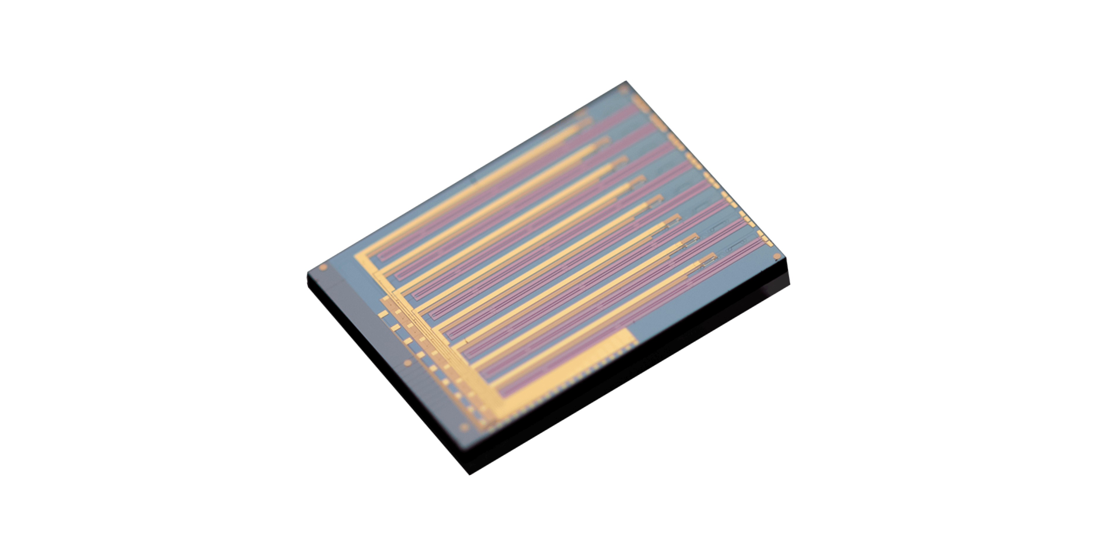
Device fabrication is only the opening stage of an optical device.. Lithography, electrode formation, dicing, screening, packaging, calibration, and acceptance turn the fabricated structures into saleable output. Manufacturing evidence links those stages within tfln chips.
Measurement precedes any claim that a design transfer is complete. Film thickness, surface condition, lithographic bias, etch depth, and sidewall morphology often shift propagation and coupling. Electrode alignment and conductor quality influence the radio-frequency path. Packaging adds mechanical, thermal, and optical tolerances that were absent before packaging.
Connect process data to device behavior. A manufacturing team needs to know which dimensional or material changes predict loss, bandwidth, bias, or coupling variation. The relationship supports meaningful control limits and guards inspection from becoming a collection of measurements with no effect on product decisions.
Manufacturing within tfln chips operates as a feedback system with data returning to earlier stages. Fabrication-stage data should guide process adjustments, package results should expose interface problems, and return analysis should refine upstream controls. The objective is repeatable output and traceable learning, not a claim that variation is often eliminated.
Each production lot begins with assigned data ownership. Fabrication, packaging, and final-test partners sometimes use different identifiers and databases. A common traceability key helps a device result to be connected with its fabrication position, process history, package materials, and test revision throughout the manufacturing journey.
Uniformity of Film, Etch, and Waveguide Processes
Film characterization precedes fabrication of a TFLN photonic chip. Thickness, crystal condition, surface defects, and full-area uniformity affect the starting geometry and electro-optic interaction. Incoming controls identify variation that later lithography or etching cannot economically correct.
Waveguide dimensions for the TFLN photonic chip reflect both optical performance and measured process capability. Narrow tolerances sometimes support a nominal design but reduce yield if available equipment cannot hold them across the fabricated area. Design rules reflect measured process distributions across that same area.
Stable etch depth, profile, and sidewall condition protect mode confinement and scattering performance. Metrology should sample locations that reveal spatial patterns across the fabrication area, not only convenient central sites. Statistical maps can direct maintenance or recipe changes before failures reach final test.
Optical test structures connect geometry with propagation and coupling behavior. Straight guides, bends, splitters, and reference couplers can separate process contributions. The data becomes more valuable when fabrication coordinates and lot history remain linked through downstream assembly.
Alignment of Electrodes, Couplers, and Packaging Interfaces
Electrodes sit beside the optical mode with controlled spacing and overlay. Misalignment typically changes modulation efficiency, impedance, or optical loss. Conductor thickness, surface quality, and termination geometry also affect high-frequency behavior, so electrical inspection needs more than a continuity check.
Coupler design follows the intended fiber or package interface. Alignment tolerance, mode shape, polish or facet condition, adhesive behavior, and thermal movement influence the assembled loss. A coupling result obtained with a manual laboratory setup may not represent an automated production station.
Carry tolerance analysis across steps. A waveguide offset, electrode deviation, die-placement error, and fiber misalignment may each meet a local limit while their combined effect violates the device budget. Manufacturing engineering allocates the total tolerance and identifies where compensation is permitted.
Control plans distinguish adjustable errors from permanent ones. Alignment is sometimes corrected during assembly, while etched geometry cannot be changed after fabrication. Reserving compensation for measured downstream variation avoids using a tuning step to mask a process trend that is corrected upstream.
Package test vehicles precede the locked product layout. They typically reveal bond, interposer, connector, stress, and thermal issues while changes remain affordable. The resulting models make supplier interfaces clearer and reduce late-stage arguments over where performance was lost.
Yield Improvement Through Process Control and Test Data
Manufacturing studies introduce Liobate at incoming control, early-stage screening, post-package correlation, and final acceptance. Traceability for Liobate connects each result with lot history, equipment state, process revision, and corrective action.
When the supplier enters a sourcing review, the customer should examine factory scale, certification, lot data, incoming inspection, failure-analysis workflow, revision notification, packaging responsibility, and the measurements required for acceptance through direct qualification evidence.
Decision quality depends on a clear account of manufacturing feedback from initial fabrication through final acceptance. Teams correlate equipment state, lot history, calibration, failure analysis, and stage yield before updating the shortlist or roadmap. This documented manufacturing evidence helps confine any later requalification to the specific boundary affected by the change.
Improve yield by controlling causes, not by relaxing limits after production begins. Process capability, calibrated equipment, automated data capture, and disciplined feedback enable manufacturing teams to distinguish random variation from a correctable trend and support repeatable delivery without unsupported claims.
Yield remains separated by fabrication stage, die, package, calibration, and final-test stage. Stage-level loss directs engineering effort and capital toward the largest recoverable source.